
最后编辑于: 2010-04-01 21:28 | 分类: 电子 | 标签: | 浏览数: 2534 | 评论数: 0
转自wikipedia:http://en.wikipedia.org/wiki/Open_collector
An open collector is a type of output on many integrated circuits (IC). Instead of outputting a signal of a specific voltage or current, the output signal is applied to the base of an internal NPN transistor whose collector is externalized (open) on a pin of the IC. The emitter of the transistor is connected internally to the ground pin. If the output device is a MOSFET the output is called open drain and it functions in a similar way.
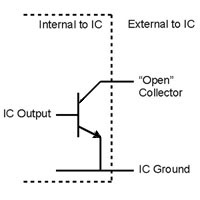
A simplified schematic of the externalized (open) collector of an integrated circuit (IC).
In the picture above, the transistor base is labeled "IC Output". This is an internal output from the internal IC logic to the transistor. From the point of view of the transistor, this is the input which controls the transistor switching. The external output is the transistor collector, and the transistor acts as an interface between the internal IC logic and parts external to the IC.
The output essentially acts as either an open circuit (no connection to anything) or a short circuit to ground. This is then usually connected to an external pull-up resistor, which sets the output to a voltage of line to which it is pulled-up when the transistor is opened. When any transistor connected to this resistor is closed, the output is forced to 0 volts. Open-collector outputs can be useful for analog weighting, summing, limiting, etc., but such applications are not discussed here.
One useful property is that the pull-up resistor need not be connected to a voltage similar to that of the chip supply (Vcc); a lower or higher voltage can be used instead. Open collector circuits are therefore sometimes used to interface different families of devices that have different operating logic voltage levels or to control external circuitry that requires a higher voltage level (e.g. a 12 V relay).
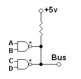
Another advantage is that more than one open-collector output can be connected to a single line. If all outputs attached to the line are in the high-impedance (i.e., logic 1) state, the pull-up resistor will hold the wire in a high voltage state. If 1 or more of the device outputs are in the ground (i.e., logic 0) state, they will sink current and pull the line voltage near ground. Open-collector devices are commonly used to connect multiple devices to a bus (i.e., one carrying interrupt or write-enable signals). This enables one device to drive the bus without interference from the other inactive devices - if open-collector devices are not used, then the outputs of the inactive devices would attempt to hold the bus voltage high, resulting in unpredictable output.
By tying the output of several open collectors together, the common line becomes a "wired AND" (positive-true logic) or "wired OR" (negative-true logic) gate. A "wired AND" behaves like the boolean AND of the two (or more) gates in that it will be logic 1 whenever (all) are in the high impedance state, and 0 otherwise. A "wired OR" behaves like the boolean OR for negative-true logic, where the output is LOW if any one of its inputs is low. Such circuit constructions are termed "wired-AND" and "wired-OR", respectively.
One problem with open-collector devices is power consumption, as they tend to require higher current minimums for correct operation. Even in the 'off' state, they often have a few nanoamps of leakage current (the exact amount varies with temperature).
SCSI-1 devices use open collector for electrical signaling. 1 SCSI-2 and SCSI-3 may use EIA-485.
Active-low wired-OR / active-high wired-AND circuit using open-drain gates.
The word "drain" in the term "Open-drain" refers to the drain terminal of a MOSFET. (The analogous term for BJT devices is open collector.) Open-drain outputs can be useful for analog weighting, summing, limiting, etc., but only applications in digital logic will be discussed. An open drain terminal is connected to ground in the low voltage (logic 0) state, but has high impedance in the logic 1 state. This prohibits current flow, but as a result, such a device requires an external pull-up resistor connected to the positive voltage rail (logic 1).
Note that microelectronic devices using open drain signals (such as microcontrollers) may provide a 'weak' internal pull-up resistor to connect the terminal in question to a positive voltage source/rail like Vdd of the device. Such weak pullups, often on the order of 100 KOhms, reduce power usage by keeping input signals from floating. External pullups are stronger (perhaps 3 KOhms) to reduce signal rise times (as with I2C) or to minimize noise (as on system RESET inputs). Internal pullups can often be disabled for cases where there is an external one, or in other cases where they are not needed.